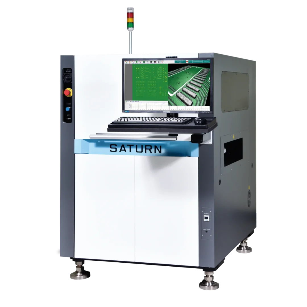
Three-dimensional solder paste inspection, or 3D SPI, measures solder paste deposits after stencil printing or dispensing. It helps manufacturers evaluate characteristics such as deposit height, area, volume and position before components are placed on the board.
This early inspection step is useful because printing variation can lead to soldering defects later in the SMT process. Fine-pitch pads and small apertures require particular attention to deposit consistency. Measurement results can help distinguish insufficient paste, excessive deposits and alignment issues when interpreted against the board’s intended design.
Select a system around the smallest features to be measured, required inspection speed and PCB dimensions. Accurate pad data and appropriate thresholds are important for avoiding unnecessary review. Where supported, communication between SPI and the printer can assist process adjustment, while stored results help trace repeated printing problems.
Explore 3D SPI systems at Sinerji. Our team can help you find solder paste inspection equipment suited to your printing process and SMT quality requirements.
Pemtron develops advanced inspection solutions based on its proprietary 3D precision measurement technology. Its 3D SPI and 3D AOI systems serve SMT and electronics manufacturing, supported by X-ray, wire bond, and coating inspection equipment. Pemtron enhances accuracy, quality control, and process reliability across semiconductor and automotive industries.

 English
 Türkçe