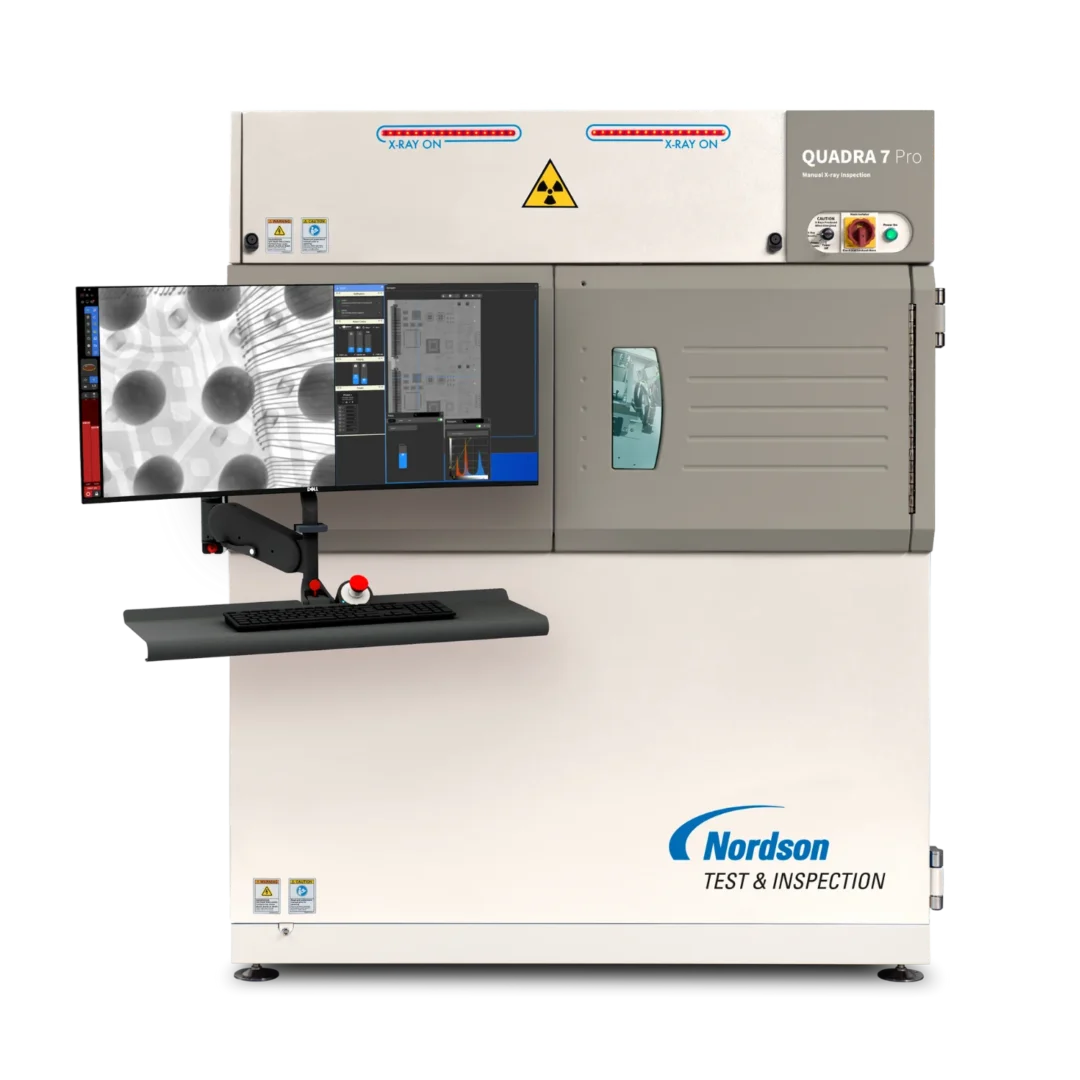
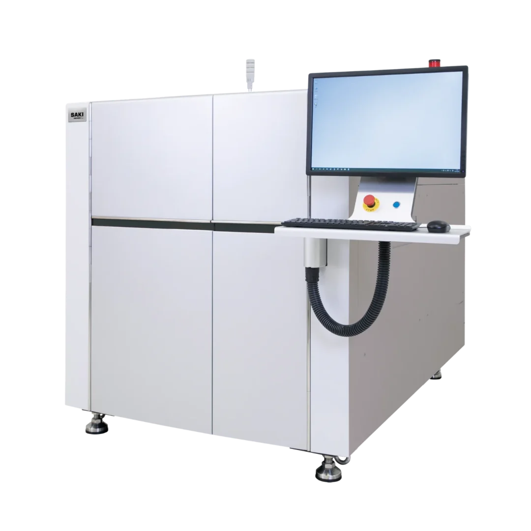
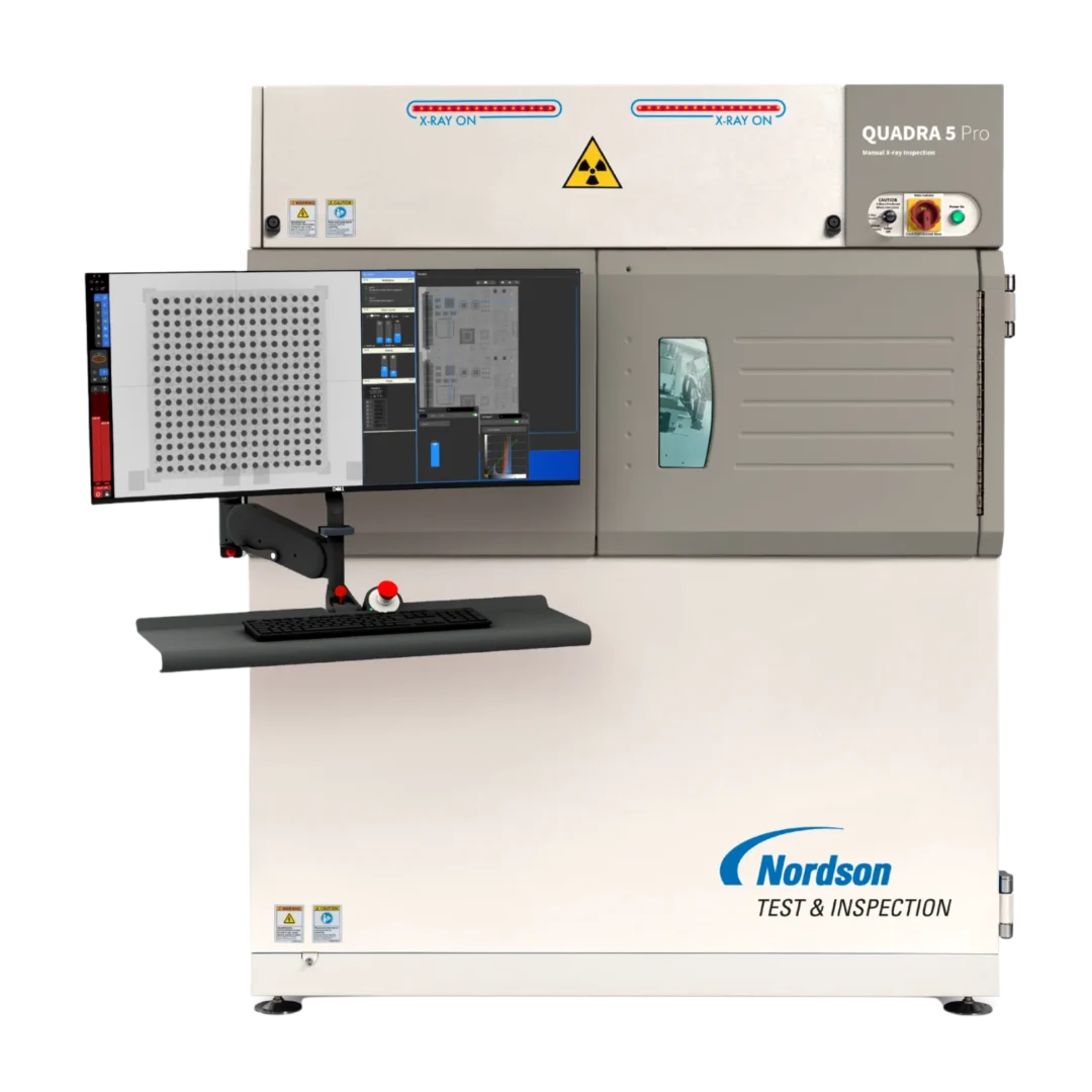
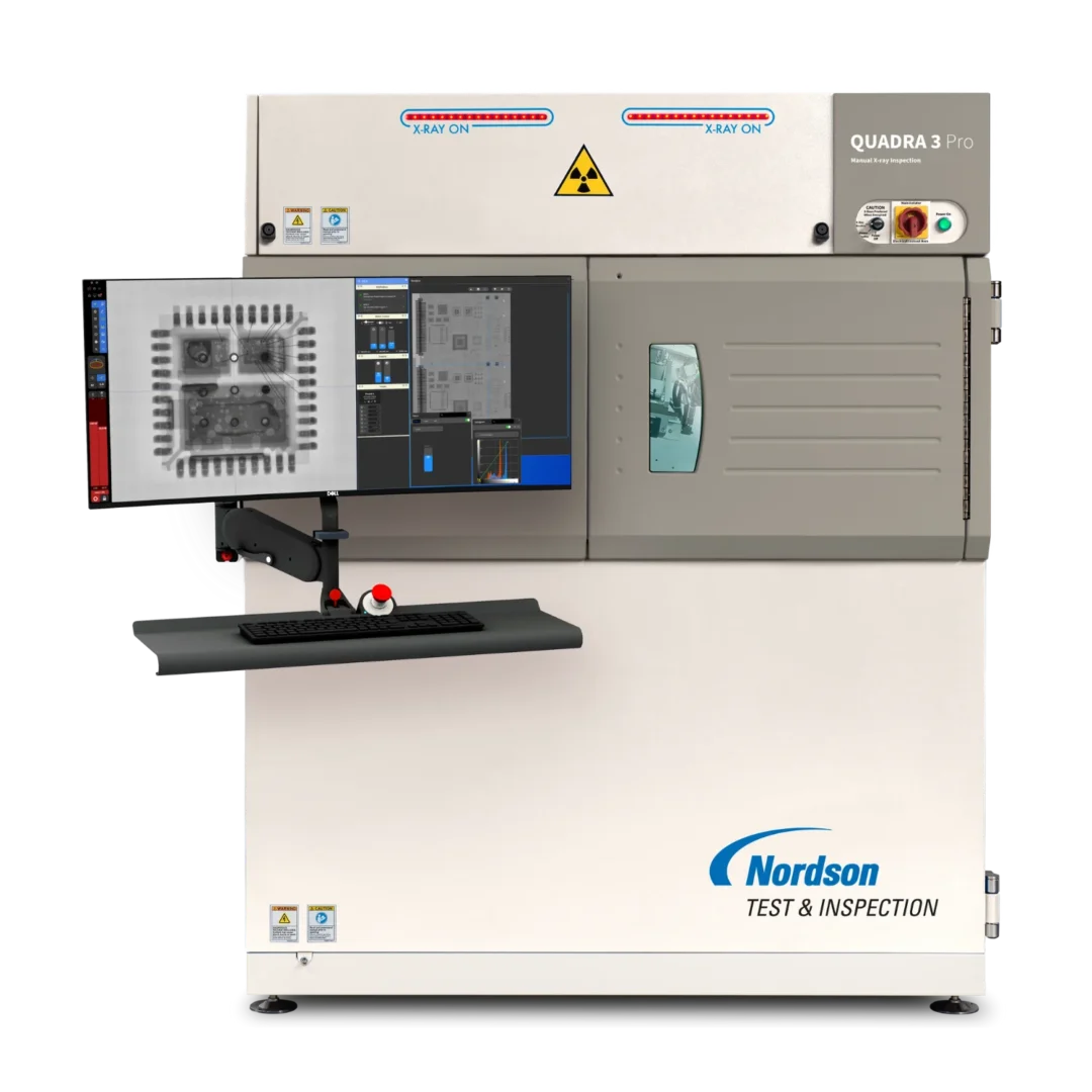
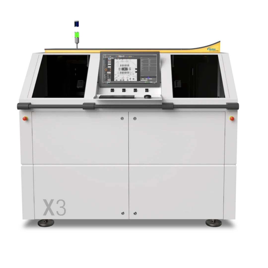
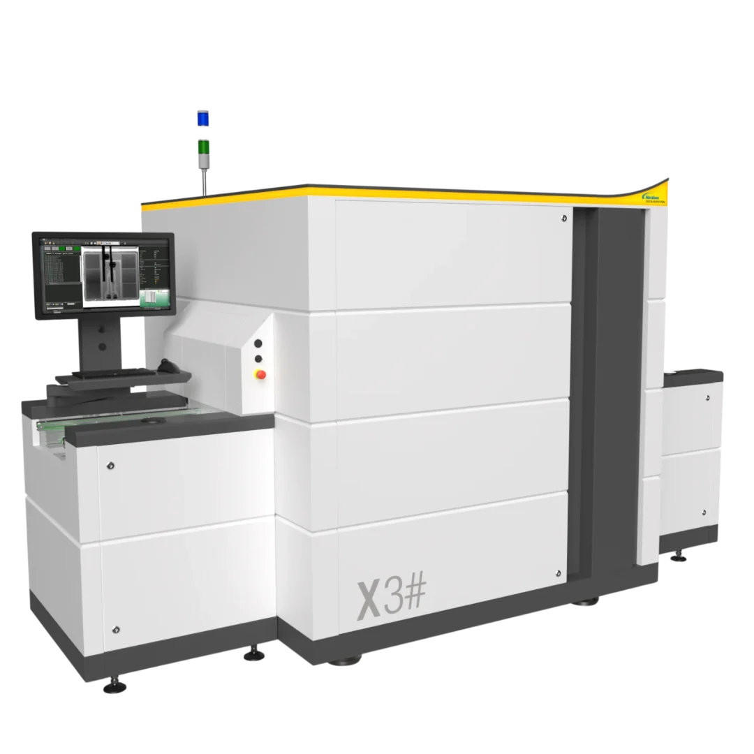
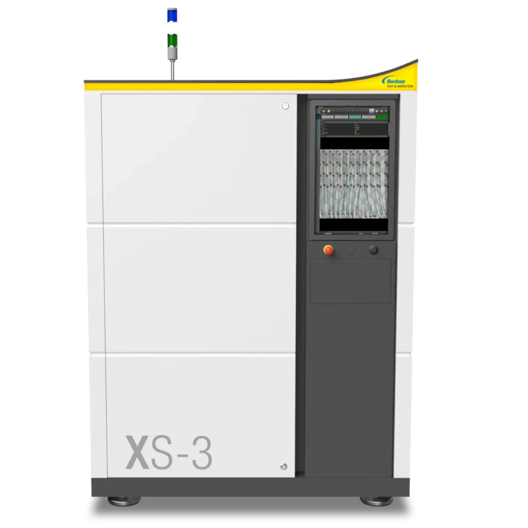
X-ray inspection systems reveal features that are hidden from ordinary optical inspection. In electronics manufacturing, they are used to examine solder joints beneath BGAs and other packages, as well as internal structures in suitable components and assemblies.
X-ray images can help assess solder joint voiding, connection geometry and selected assembly defects. Two-dimensional imaging and computed tomography provide different views, so the inspection method should match the structure being investigated. Image interpretation requires suitable views and an understanding of the sample.
Compare resolution, sample size, access angles and inspection speed against your actual applications. Dense materials and fine features may require different imaging conditions. Manual analysis is valuable for troubleshooting, while automated inspection can support repeatable checks where the application permits. Recorded images provide useful evidence when comparing assemblies or investigating a process change.
Sinerji offers X-ray inspection equipment for electronic assemblies. Contact our team to identify suitable imaging capabilities for your packages, PCB designs and quality-analysis needs.



 English
 Türkçe